Showing posts with label IC555 Timer circuits. Show all posts

Monday, June 27, 2011

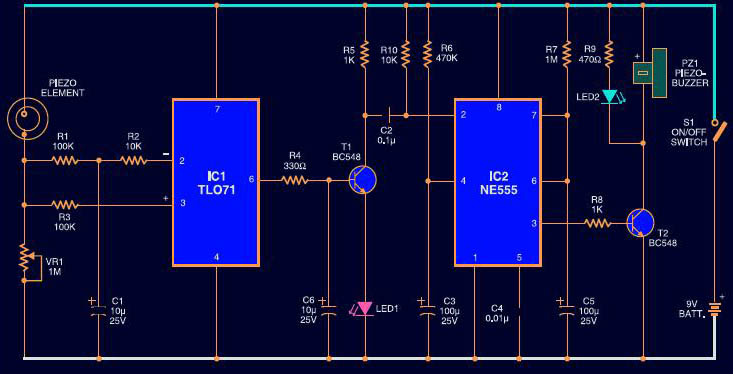
Animal or Human Vibration Security Sensor


This circuit simulates a seismic sensor to detect vibrations/ sounds. It is very sensitive and can detect vibrations caused by the movement of animals or human beings. So it can be used to monitor protected areas to restrict entry of unwanted persons or animals.
click to enlarge

  The circuit uses readily available components and the design is straightforward. A standard piezo sensor is used to detect vibrations/sounds due to pressure changes. The piezo element acts as a small capacitor having a capacitance of a few nanofarads. Like a capacitor, it can store charge when a potential is applied to its terminals. It discharges through VR1, when it is disturbed. In the circuit, IC TLO71 (IC1) is wired as a differential amplifier with both its inverting and non-inverting inputs tied to the negative rail through a resistive network comprising R1, R2 and R3. Under idle conditions (as adjusted by VR1), both the inputs receive almost equal voltages, which keeps the output low.
TLO71 is a low-noise JFET input op-amp with low input bias and offset current. The BIFET technology provides fast slew rates. Capacitor C1 is provided in the circuit to keep the differential input of IC1 for better performance. When the piezo element is disturbed (by even a slight movement), it discharges the stored charge.
 This alters the voltage level at the inputs of IC1 and the output momentarily swings high as indicated by green LED1. This high output is used to trigger switching transistor T1, which triggers monostable IC2. The timing period of IC2 is determined by R7 and C5. With the shown values, it will be  around two minutes. The high output from IC2 activates T2 and the buzzer starts beeping along with red light indication from LED2.
  Assemble the circuit on a common PCB and enclose in a suitable cabinet. Connect the piezo element to the PCB using single-core shielded wire. Enclose the piezo element inside a rustproof, small aluminium box. The piezo element should be firmly glued to the enclosure facing the fine side towards the case. Fix the sensor assembly on the back side of a ceramic tile or granite tile with good adhesive. Fix the tile (or bury it in the earth) near the entrance with the sensor assembly facing downwards. Whenever a pressure change develops near the sensor, the circuit will be activated.

Voltage Doubler To 6v


All miniature electronic devices operate off batteries. Some of them need higher than the standard battery voltages to operate efficiently. If the battery of that specific voltage is unavailable, we are forced to connect additional cells in series to step up the DC voltage. Thus,
the true meaning of miniaturisation is lost. A simple way to overcome this problem is to employ a voltage doubler, if the device under consideration can operate at a small current.
 Here we present a low-power voltage doubler circuit that can be readily used with devices that demand higher voltage than that of a standard battery but low operating current to work with. The circuit is quite simple as it uses only a few components. Yet, the output efficiency is 75 to 85 per cent along its operating voltage range. The available battery voltage is almost doubled at the output of the circuit. Here IC1 is wired as an astable multivibrator to generate rectangular pulses at around 10 kHz. This frequency and duty cycle of the pulses can be varied using preset VR1. The pulses are applied to switching transistors T1 and T2 for driving the output section, which is configured as a voltage-doubling circuit. The doubled voltage is available across capacitor C5.
 During each cycle of the pulse occurance, the high level drives T1 into its saturation, keeping transistor T2 cut off. So transistor T1 charges capacitor C4 via the path formed by diodes D2 and D1 to a voltage level slightly lesser than the supply. But during the low period of the pulse, transistor T1 is cut off while transistor T2 is driven into saturation. Now, transistor T2 raises the charge on the negative pole of capacitor C4 by another step equal to the supply voltage. Therefore an equal amount of charging is built up on capacitor C5 via diode D3. This doubling action increases the total voltage across capacitor C5 to almost double the input voltage. If the output of the pulse generator is maintained with a high enough amplitude and frequency, the output voltage and current remain constant and cater to the needs of the load.
click to enlarge

  Even with the half-wave function, this circuit is almost free of ripple voltage. If the connected load doesn’t require a high current, the efficiency can be expected in the upper 90 per cent ranges. Since the input voltage is doubled, the current drain from the input power supply is also doubled at the input but halved at the output. One point of caution is that if the multivibrator’s frequency is fairly high, the output may suffer with the interference imposed over the DC voltage. In this case, the frequency must be set favourably by trials and actual load connection procedure. This tiny circuit can be assembled on the general-purpose PCB. If all of the components are surface-mount type, the whole module can be genuinely miniaturised.
  During testing with input of 8V and 1.25mA load current the output voltage was found to be around 13V.

Remote control Timer


This infrared remote control timer can be used to turn an appliance on/off for a period of 0.11 second to 110.0 seconds. 
click to enlarge

The circuit comprises two sections, namely, the transmitter section and the receiver section.
Fig. 1 shows the IR transmitter section. The astable multivibrator NE555 (IC1) is used to  enerate a 10kHz modulated IR signal. The output of IC1 is connected to the base of pnp transistor T1 via resistor R2. Two infrared LEDs (IR1 and IR2) are connected in series between the collector (via resistor R3) and ground. When switch S1 is pressed, the IR LEDs transmit the modulated IR signal of 10-11 kHz. This frequency can be changed with the help of VR1 potmeter.
  In the receiver section shown in Fig. 2, two photodiodes (IR3 and IR4) receive the IR sign l transmitted by the IR transmitter. Transistors T2 and T3 amplify the weak signal. The amplified signal is filtered by capacitors C6 and C7. The amplified and filtered signal is now fed to the inverting input pin 2 of op-amp IC2 (IC 741). The output of IC2 is further connected to trigger pin 2 of timer NE555 (IC3) that is used as a monostable multivibrator whose frequency may be varied with the help of potmeter VR3.
  When switch S1 of the transmitter is pressed, the modulated IR rays are generated, which are received by photodiodes in the receiver section and amplified by the amplifier circuit. The output of op-amp goes low to trigger the monostable. Then high output at pin 3 of IC3 activates the twochangeover relay RL via transistor T3 (BC548) for a preset time.
  The on/off time can be set in the timer with the help of VR3 and C0. Switch S2 is used to reset the monostable. If you want to turn the appliance on for a preset time, connect the appliance via relay RL(a). On the other hand, if you want to turn the appliance off for a preset time, connect the appliance via relay RL(b). The timer can be reset by pressing reset switch S2.
 The circuit works up to 3 metres without using any focusing lens. However, you can increase the operating range by using focusing lens

Sensor Night Lamp With Morning Alarm


This circuit automatically turns on a night lamp when bedroom light is switched off. The lamp remains ‘on’ until the light sensor senses daylight in the morning. A super-bright white LED is used as the night lamp. It gives bright and cool light in the room. When the sensor detects the daylight in the morning, a melodious morning alarm sounds. 
Click to enlarge

 The circuit is powered from a standard 0-9V transformer. Diodes D1 through D4 rectify the AC voltage and the resulting DC voltage is smoothed by C1. Regulator IC 7806 gives regulated 6V DC to the circuit. A battery backup is provided to power the circuit when mains fails. When mains supply is available, the 9V rechargeable battery charges via diode D5 and resistor R1 with a reasonably constant current. In the event of mains failure, the battery automatically takes up the load without any delay. Diode D5 prevents the battery from discharging backwards following the mains failure and diode D6 provides current path from the battery.
 The circuit utilises light-dependant resistors (LDRs) for sensing darkness and light in the room. The resistance of LDR is very high in darkness, which reduces to minimum when LDR is fully illuminated. LDR1 detects darkness, while LDR2 detects light in the morning. The circuit is designed around the popular timer IC NE555 (IC2), which is configured as a monostable. IC2 is activated by a low pulse applied to its trigger pin 2. Once triggered, output pin 3 of IC2 goes high and remains in that position until IC2 is triggered again at its pin 2. When LDR1 is illuminated with ambient light in the room, its resistance remains low, which keeps trigger pin 2 of IC2 at a positive potential. As a result, output pin 3 of IC2 goes low and the white LED remains off. As the illumination of LDR1’s sensitive window reduces, the resistance of the device increases.
 In total darkness, the specified LDR has a resistance in excess of 280 kiloohms. When the resistance of LDR1 increases, a short pulse is applied to trigger pin 2 of IC2 via resistor R2 (150 kiloohms). This activates the monostable and its output goes high, causing the white LED to glow. Low-value capacitor C2 maintains the monostable for continuous operation, eliminating the timer effect. By increasing the value of C2, the ‘on’ time of the white LED can be adjusted to a predetermined time.
LDR2 and associated components generate the morning alarm at dawn. LDR2 detects the ambient light in the room at sunrise and its resistance gradually falls and transistor T1 starts conducting. When T1 conducts, melody-generator IC UM66 (IC3) gets supply voltage from the emitter of T1 and it starts producing the melody. The musical tone generated by IC3 is amplified by single-transistor amplifier T2. Resistor R7 limits the current to IC3 and zener diode ZD limits the voltage to a  afer level of 3.3 volts.
 The circuit can be easily assembled on a general-purpose PCB. Enclose it in a good-quality plastic case with provisions for LDR and LED. Use a reflective holder for white LED to get a spotlight effect for reading. Place LDRs away from the white LED, preferably on the backside of the case, to avoid unnecessary illumination. The speaker should be small so as to make the gadget compact.

Highway Alert signal Generator


Here is a signal lamp for safe highway driving. The lamp automatically emits brilliant tricolour light when a vehicle approaches the rear side of your vehicle. It emits light for 30 seconds that turns off when the approaching vehicle overtakes. The ultra-bright blue, white and red LEDs of the signal lamp emit very bright light to alert the approaching vehicle’s driver even during the day, giving additional safety during night, or when you need to stop your vehicle on side of the highway.
click to enlarge

 The circuit saves considerable battery power. The circuit is built around two timer ICs NE555 (IC1 and IC2). IC1 is designed as a standard monostable, while IC2 is designed as an astable. Darlington phototransistor L14F1 (T1) is used as a photosensor to activate the monostable. The collector of phototransistor T1 is connected to trigger pin 2 of IC1, which is normally kept high by resistor R1.
  When headlight from an approaching vehicle illuminates the phototransistor, it conducts to give a short pulse to IC1, and the output of IC1 goes high for a period determined by resistor R2 and capacitor C1. The output of IC1 is fed to the base of transistor T2 via resistor R3. Transistor T2 conducts to drive transistor T3 and its collector goes high to take reset pin 4 of IC2 to high level. This activates astable IC2, which switches on and off the LED chain alternately. The intermittent flashing of LEDs gives a beautiful tricolour flashlight effect.
 The circuit can be easily constructed on a small piece of general-purpose PCB. Fig. 2 shows the bottom and front views of Darlington phototransistor L14F1. The proposed arrangement of LEDs, which are soldered in a circular fashion on a general purpose PCB, is shown in Fig. 3. Use a circular reflector for the LEDs to get brighter light. Fix the LED arrangement on the rear side of your vehicle, and the phototransistor where it is illuminated directly by the headlight of the approaching vehicle. 12V DC supply to the circuit, can be provided by your vehicle battery with proper polarity.

Vehicle Break Failure Indicator


Do you want to get an early warning of brake failure while driving? Here is a brake failure indicator circuit that constantly monitors the condition of the brake and gives an audio-visual indication. When the brake is applied, the green LED blinks and the piezobuzzer beeps for around one second if the brake system is intact. If the brake fails, the red LED glows and the buzzer stops beeping. 
click to enlarge

 The circuit will work only in vehicles with negative grounding. It also gives an indication of brake switch failure.
 In hydraulic brake systems of vehicles, a brake switch is mounted on the brake cylinder to operate the rear brake lamps. The brake switch is fluidoperated and doesn’t function if the fluid pressure drops due to leakage. The fluid leakage cannot be detected easily unless there is a severe pressure drop in the brake pedal. This circuit senses the chance of a brake failure by monitoring the brake switch and reminds you of the condition of the brake every time the brake is applied.
 The circuit uses an op-amp IC CA3140 (IC2) as voltage comparator and timer NE555 (IC3) in monostable configuration for alarm. Voltage comparator IC2 senses the voltage level across the brake switch. Its non-inverting input (pin 3) gets half the supply voltage through potential divider resistors R3 and R4 of 10 kilo-ohms each. The inverting input (pin 2) of IC2 is connected to the brake switch through diode D1, IC 7812 (IC1) and resistor R2. It receives a higher voltage when the brake is applied.
 Normally, when the brake is not applied, the output of IC2 remains high and the red LED (LED1) glows. The output of IC2 is fed to trigger pin 2 of the monostable through coupling capacitor C2. Resistor R1 is used for the input stability of IC2. IC1 and C1 provide a ripple-free regulated supply to the inverting input of IC2. IC3 is wired as a monostable to give pulse output of one second. Timing elements R7 and C4 make the output high for one second to activate the buzzer and LED2. Usually, the trigger pin of IC3 is high due to R6 and the buzzer and LED2 remain ‘off.’
 When the brake pedal is pressed, pin 2 of IC2 gets a higher voltage from the brake switch and its output goes low to switch off the red LED. The low output of IC2 gives a short negative pulse to the  monostable through C2 to trigger it. This activates the buzzer and LED2 to indicate that the brake system is working. When there is pressure drop in the brake system due to leakage, LED1 remains ‘on’ and the buzzer does not sound when the brake is applied. The circuit can be assembled on any general-purpose PCB or perforated board. Connect point A to that terminal of the brake switch which goes to the brake lamps. The circuit can be powered from the vehicle’s battery.
  The circuit requires well-regulated power supply to avoid unwanted triggering while the battery is charging from the dynamo. IC4, C6 and C7 provide regulated 12V to the circuit. The power supply should be taken from the ignition switch and the circuit ground should be clamped to the vehicle’s body. A bicolour LED can be used in place of LED1 and LED2 if desired.

security counter for Doors


This simple circuit produces a warning beep when somebody crosses a protected area in your home or office. The switch, hidden below the floor mat, triggers the alarm when the person walks over it. 
click to enlarge

 The circuit uses a conductive foam as the switch. It can be two small pieces of conductive pads usually used to pack sensitive ICs as antistatic cover. Alternatively, you can make the switch by coating conducting carbon ink on two small pieces of a copper-clad board. When the circuit is in standby mode, transistor T1 does not conduct, since its base is floating.
 When the person walks, the switch is pressed and current flows through R1 and the switch to provide positive bias to transistor T1. Transistor T1 conducts and its collector voltage drops, which acts as a negative trigger input for the monostable wired around IC NE555 (IC1). IC1 outputs a pulse of fifty-seconds duration with preset values of R4 and C3. This pulse is applied to the buzzer through transistor T2. The buzzer sounds a warning beep on unauthorised entry. The pulse duration can be changed to the desired value by changing the values of R4 and C 3 . Resistor R2 in the circuit makes the trigger pin of IC1 high to prevent false triggering.
 Assemble the circuit on a generalpurpose PCB and enclose in a plastic case. Use a 9V battery to power the circuit. Connect the touchpad switch with the PCB and hide under the mat at the entrance. The PCB can be mounted on the nearby wall. Make the switch carefully using conducting foam or copper clad coated with conducting ink. Place the two pieces with their conducting surface facing each other. Solder carefully a thin copper electric wire and ensure that it makes contact when the two plates touch together on pressing. Provide two 1cm rubber tabs between the plates to avoid touch in the standby mode.

Sunday, June 19, 2011

SPELLER EFFECT SIGN DISPLAY


The circuit described here uses lowcost and easily available IC CD4017 to produce a speller type light display. In such displays, each letter of the sign sequentially lights up, one after the other, until all letters are glowing. After a few seconds, the letters switch off and the cycle repeats. This circuit provides a maximum of nine channels and therefore can be used to spell a word or sign having up to nine characters. 
click to enlarge

 Timer IC1 (555) is configured in astable mode to produce clock signal for triggering IC2 (CD4017). Speed of switching on the display can be controlled by varying preset VR1.
  CD4017 is a decade counter having ten outputs, of which one output is high for each clock pulse. However, this produces running lights effect. To change this sequence to get the speller effect, pnp transistors T1 through T9 are wired as shown in the figure. Nine triacs (triac 1 through triac 9) are used to drive 230V bulbs. (In place of 230V bulbs, miniature lamps  connected in series in the form of characters or letters can also be used, provided the voltage drop across the series combination is 230 volts.)
 When any of the outputs of IC2 goes high, the corresponding transistor connected to the output goes off. When Q0 is high, transistor T1 goes off and its output at the collector goes low. Since the emitter of transistor T2 is connected to the collector of transistor T1, and collector and emitter terminals of transistors T1 through T9 are connected in series, all transistors next to transistor T1, i.e. transistors T2 through T9, do not get supply and hence all their outputs go low.
  Next, when Q1 output goes high, transistor T2 goes off. Thus outputs of transistors T2 through T9 remain low. Since Q0 output at this instant is low, transistor T1 is forward biased and its output goes high to light up the first character.
 Similarly, when Q2 output goes high, Q0 and Q1 outputs are low and therefore outputs of transistors T1 and T2 go high to light up the first and second characters.
 This process continues until all transistors turn on, making all the characters to light up. The cycle repeats endlessly, producing the speller type light effect.

Smart Vibration Sensor


In this vibration sensor alarm circuit, initially, when power switch S1 is flipped to ‘on’ position, power indicator LED1 lights up immediately. IC LM555 (IC1), wired as a simple latch circuit with control input, is powered and R-C components R4 and C5 connected at its reset pin 4 force the latch to standby mode (with inactive low output). The circuit is driven into sleep mode.
CLICK TO ENLARGE

 As soon as vibration is detected, MOSFET T1 is fired by the positive going pulse output from the vibration sensing mechanism built around piezo-ceramic wafer and associated components. As a result, control input pins 2 and 6 of IC1 latch are grounded. Output pin 3 of IC1 now goes high. The positive supply from output pin 3 of IC1 is extended to three-tone siren generator UM3561 (IC2) through R5, D1 and R6. Components R6 and ZD1 stabilise the input power supply of IC2 to around 3.3V. Output signals from IC2 are amplified by Darlington-pair
transistors T2 and T3 to produce alert tone (police siren sound) via loudspeaker LS1.
 Reset switch S1 can be used to switch off the alarm sound by resetting the latch circuit. For safety, use key-lock type switches for S1 and S2. A relay can also be connected at the output socket (SOC1) of the circuit to energise highpower beacons, emergency sirens and fence electrification units.
 The circuit works off 9V DC. A compact PP3-/6F22-type alkaline battery can be used to power the circuit.

MOBILE CELLPHONE CHARGER


Charging of the cellphone battery is a big problem while travelling as power supply source is not generally accessible. If you keep your cellphone switched on continuously, its battery will go flat within five to six hours, making the cellphone useless. A fully charged battery becomes necessary especially when your distance from the nearest relay station increases. Here’s a simple charger that replenishes the cellphone battery within two to three hours. 

click to enlarge

 Basically, the charger is a current-limited voltage source. Generally, cellphone battery packs require 3.6-6V DC and 180- 200mA current for charging. These usually contain three NiCd cells, each having 1.2V rating. Current of 100mA is sufficient for charging the cellphone battery at a slow rate. A 12V battery containing eight pen cells gives sufficient current (1.8A) to charge the battery connected across the output terminals. The circuit also monitors the voltage level of the battery. It automatically cuts off the charging process when its output terminal voltage increases above the predetermined voltage level.
 Timer IC NE555 is used to charge and monitor the voltage level in the battery. Control voltage pin 5 of IC1 is provided with a reference voltage of 5.6V by zener diode ZD1. Threshold pin 6 is supplied with a voltage set by VR1 and trigger pin 2 is supplied with a voltage set by VR2. When the discharged cellphone battery is connected to the circuit, the voltage given to trigger pin 2 of IC1 is below 1/3Vcc and hence the flip-flop in the IC is switched on to take output pin 3 high.
 When the battery is fully charged, the output terminal voltage increases the voltage at pin 2 of IC1 above the trigger point threshold. This switches off the flip-flop and the output goes low to terminate the charging process. Threshold pin 6 of IC1 is referenced at 2/3Vcc set by VR1. Transistor T1 is used to enhance the charging current. Value of R3 is critical in providing the required current for charging. With the value of 39-ohm the charging current is around 180 mA.   
  The circuit can be constructed on a small general-purpose PCB. For calibration of cut-off voltage level, use a variable DC power source. Connect the output terminals of the circuit to the variable power  supply set at 7V. Adjust VR1 in the middle position and slowly adjust VR2 until LED1 goes off, indicating low output. LED1 should turn on when the voltage of the variable power supply reduces below 5V. Enclose the circuit in a small plastic case and use suitable connector for connecting to the cellphone battery.
Note., the circuit was tested with a Motorola make cellphone battery rated at 3.6V, 320 mAH. In place of 5.6V zener, a 3.3V zener diode was used. The charging current measured was about 200 mA.The status of LED1 is shown in the table.

Low-Cost PCO Billing Meter


The circuit presented here can be used in PCOs for displaying the actual bill. The comparative disadvantages of the presented circuit are as follows:

click to enlarge

1. The calculator used along with thiscircuit is required to be switched ‘on’ manually before making a call.
2. Certain manual entries have to be made in the calculator; for example, for a pulse rate of Rs 1.26, number 1.26 is to be entered after switching ‘on’ the calculator followed by pressing of ‘+’
button twice. However, possibility exists for automating these two functions by using additional circuitry.
  In telephony, on-hook condition is represented by existance of 48V to 52V across the line. Similarly, the off-hook condition is represented by the line voltage dropping to a level of 8V to 10V (depending upon the length of the local lead line (local loop) from telephone exchange to the subscriber’s premises as well as upon the impedance of telephone instrument). Handset is normally lifted either for dialing or in response to a ring.
  In the circuit shown in Fig. 1, when
the handset is off-hook, the optocoupler MCT2E (IC1) conducts and forward biases transistor T1, which, in turn, forward biases transistor T2 and energises relay RL1. In energized condition of relay, the upper set of relay contacts connects the positive supply rail to PLL (phaselocked loop) IC2 (LM567) pin 4, while the lower set of relay contacts couples the positive telephone lead to input pin 3 of LM567 via capacitor C1 and resistor R3.
 The negative telephone lead is pe- rmanently capacitively coupled to ground via capacitor C2. As soon as call matures, 16kHz tone pulses would be pumped into the telephone line by the telephone exchange at suitable intervals. This interval depends on the pulse rate of the place called and also the time of the day and whether it’s a working-day or holiday. On receipt of 16kHz pulse,output pin 8 of IC LM567 (which is tuned for centre frequency of 16 kHz) goes ‘low’ for the duration of the pulse. The output of IC2 is coupled via transistor T3 to optocoupler IC3. The output of this optocoupler is used to bridge the ‘=’ button on a calculator (such as Taksun make), which has the effect of pressing the ‘=’ button of the calculator.
 Considering that pulse rate for a specific town/time/day happens to be Rs 1.26 per pulse, then before maturity of the call one enters 1.26 followed by pressing of ‘+’ key twice. Now, if a total of ten billing pulses have been received from exchange for the duration of the call, then on completion of the call, the
calculator display would show 12.60. The telephone operator has to bill the customer Rs 14.60 (Rs 12.60 towards call charges plus Rs 2.00 towards service charges).
 For tuning of the PLL circuit around IC2, lift the handset and inject 16kHz tone across the line input points. Tune IC2 to centre frequency of 16 kHz with the help of preset VR1. Proper
tuning of the PLL will cause LED (D6) to glow even with a very lowamplitude 16kHz tone.
 Lab note. Arrangement used for simulating a 16kHz pulsed tone is shown in Fig. 2. Push-to-on switch is used for generation of fixed-duration pulse for modulating and switching on a 16kHz oscillator.rates, pulse codes, etc, readers are advised to go through the tariff rates and
pulse code information given in the beginning pages of telephone directories, such as MTNL.

LIGHT HOUSE


This project was designed for a model lighthouse  to flash a lamp in a simple sequence: two flashes of 2s with a short gap of 1s, followed by a longer gap of 5s before repeating the sequence.

CLICK TO ENLARGE

 The 555 timer is connected as an astable to provide clock pulses for the 4017 counter. The 4017 has ten outputs (Q0 to Q9) and each one becomes high (‘on’) in turn as the clock pulses are received. Outputs Q0, Q1, Q3 and Q4 are combined with diodes to produce the flash sequence. A transistor amplifies the current to power the lamp, or LED if you prefer (a 470W LED resistor is included on the stripboard layout). The 1MW preset controls the time period (T) of the 555 astable from about 0.1 to 1.5s, for example set T = 1s. For a different flash sequence connect the diodes to combine different 4017 outputs (Q0-Q9). If the full count from 0 to 9 is not required one of outputs can be connected to the reset input (pin 15). For example connecting Q8 (pin 9) to reset (pin 15) reduces the long gap at the end of the sequence to 3s (with T=1s).
Parts Required
• resistors: 470, 2k2, 22k, 100k • 555 timer IC, such as NE555
• capacitors: 0.1μF, 1μF 16V radial • 4017 counter IC
• diodes: 1N4148 × 4 • DIL sockets for ICs: 8-pin, 16-pin
• transistor: BC108 (or equivalent) • on/off switch
• 1M preset, horizontal • battery clip
• 6V 60mA MES lamp • 9V battery box for 6 × AA cells
• MES lampholder • stripboard: 19 rows × 21 holes

IC Controlled Emergency Light with Charger


 The circuit shown here is that of the IC controlled emergency light. Its main features are: automatic switching-on of the light on mains failure and battery charger with overcharge protection. 
click to enlarge

 When mains is absent, relay RL2 is in deenergised state, feeding battery supply to inverter section via its N/ C contacts and switch S1. The inverter section comprises IC2 (NE555)
which is used in stable mode to produce sharp pulses at the rate of 50 Hz for driving the MOSFETs.
  The output of IC3 is fed to gate of MOSFET (T4) directly while it is applied to MOSFET (T3) gate after inversion by transistor T2. Thus the power amplifier built around MOSFETs T3 and T4 functions in push-pull mode. The output across secondary of transformer X2 can easily drive a 230-volt, 20-watt fluorescent tube. In case light is not required to be on during mains failure, simply flip switch S1 to off position.
 Battery overcharge preventer circuit is built around IC1 (LM308). Its non inverting pin is held at a reference voltage of approximately 6.9 volts which is obtained using diode D5 (1N4148) and 6.2-volt zener D6. The inverting pin of IC1 is connected to the positive terminal of battery. Thus when mains supply is present, IC1 comparator output is high, unless battery voltage exceeds 6.9 volts. So transistor T1 is normally forward biased, which energises relay RL1. In this state the battery remains on charge via N/O contacts of relay RL1 and current limiting resistor R2. When battery voltage exceeds 6.9 volts (overcharged condition), IC1 output goes low and relay RL1 gets deenergised, and thus stops further charging of battery.
 MOSFETs T3 and T4 may be mounted on suitable heat sinks.

Tuesday, June 14, 2011

Staircase Light with Auto Switch-off


We are all familiar with the electrical wiring arrangement that connects an electrical bulb with two switches: one at the bottom of a staircase and the other at the top. Wiring is done such that either of the two switches can be used to switch the bulb on or off. In such a wiring arrangement, while climbing up the staircase which is in dark, the switch located at the bottom of the staircase is used to switch on the light. After you have climbed the staircase, you use the switch located there to switch off the light.

  The circuit presented here is an electronic-cum-electrical arrangement to get a similar facility as provided by the hard-wired electrical system, but you need to operate the switch only once. Whereas in the hard-wired arrangement if you forget to switch off the light once you have  traversed the staircase, light would remain ‘on, wasting energy.
  In this circuit also, we have two micro-switches—one located at the top and the other located at the bottom of the staircase—that can be pushed and released easily during climb-up from the bottom of the staircase or climbdown from the top of the staircase. With every push and release of either of the two switches, bulb L1 lights up for a preset time period of, say, 40 seconds, which is considered adequate for climbing up or going down the staircase. The bulb goes off automatically after the set 40 seconds. You can change this ‘on’ time by changing the values of resistor R7 and/or capacitor C4 depending upon your requirement.
  Switches S1 and S2 are the two micro-switches, which provide low inputs to the respective de-bouncing circuits. Each de-bouncing circuit is built around two NAND gates connected back to back. The de-bouncing circuits ensure a clean, bounce-free pulse at the output every time the micro-switch is pressed and released. The outputs from the two de-bouncing circuits are  ORed using diodes D1 and D2 (1N4001). So every time you press and release either of the micro-switches, you get a positive going pulse at the junction of the cathodes of diodes D1 and D2.
  These pulses are used to trigger the monostable circuit built around timer IC2. On the trailing edge of the pulse, the output of the monostable goes high for a time period of 40 seconds. This drives relay-driver transistor 2N2222 (T1) wired as a switch. Relay RL1 gets energised and closes N/O contacts of the relay, wired in series with the mains and the bulb (L1). Bulb L1 switches off when the relay gets de-energised after 40-second pulse period. Free-wheeling diode D4 (1N4001) protects transistor T1 against transients during relay switch-off operation.
  The circuit operates off a 9V battery, which gets connected to the circuit through ‘on’/‘off’ switch S3. You can also use regulated 9V power supply. Assemble the circuit on a  general purpose PCB and house in a small box. Connect micro-switches S1 and S2 near top and bottom of the staircase through flexible wires and bulb in the middle of the staircase.

Twitter Delicious Facebook Digg Stumbleupon Favorites More