Showing posts with label Pulse Generators. Show all posts

Monday, June 27, 2011

Signal Generator


This circuit is very useful while checking/operating counters, stepping relays, etc. It avoids the procedure of setting a switch for the required number of pulses. By pressing appropriate switches S1 to S9, one can get 1 to 9 negative- going clock pulses, respectively. 
Click to enlarge

 Schmitt trigger NAND gate N1 of IC2, resistor R1, and capacitor C1 are wired to produce clock pulses. These pulses are taken out through NAND gate N3 that is controlled by decade counter CD4017 (IC1). Initially no switch from S1 to S9 is depressed and the LED is glowing. As pins 5 and 6 of NAND gate N2 are pulled up by resistor R3, its output pin 4 goes low. This disables NAND gate N3 to take its output pin 10 to high state, and no pulse is available.
 IC1 is a decade counter whose Q outputs normally remain low. When clock pulses are applied, its Q outputs go high successively, i.e. Q0 shifts to Q1, Q1 shifts to Q2, Q3 shifts to Q4, and so on. If any one of switches S1 through S9, say, S5 (for five pulses), is momentarily depressed, pins 5 and 6 of NAND gate N2 go low, making its output pin 4 high, which fully charges capacitor C2 via diode D. At the same time, this high output of N2 enables NAND gate N3 and clock pulses come out through pin 10. These are the required number of pulses used to check our device.
 The clock pulses are fed to clock-enable pin 13 of IC1, which starts counting. As soon as output pin 1 (Q5) of IC1 turns high, input pins 5 and 6 of NAND gate N2 will also become high via switch S5 because high-frequency clock allowed five pulses during momentary pressing. This high input of N2 provides low output at pin 4 to disable NAND gate N3 and finally no pulse will be available to advance counter IC1. Before the next usage, counter IC1 must be in the standby state, i.e. Q0 output must be in the high state. To do this, a time-delay pulse generator wired around NAND gate N4, resister R4, diode D, capacitor C2, and differentiator circuit comprising C3 and R5 is used.
 When output pin 4 of NAND gate N2 is low, it discharges capacitor C2 slowly through resistor R4. When the voltage across capacitor C2 goes below the lower trip point, output pin 11 of NAND gate N4 turns high and a high-going sharp pulse is produced at the junction of capacitor C3 and resistor R5. This sharp pulse resets counter IC1 and its Q0 output (pin 3) goes high. This is represented by the glowing of LED.
 Ensure the red LED is glowing before proceeding to get the next pulse. Press any of the switches momentarily and the LED will glow. If the switch is kept pressed, the counter counts continuously and you cannot get the exact number of pulses.

Sunday, June 26, 2011

Shortwave Transmitter


This low-cost short-wave transmitter is tunable from 10 to 15 MHz with the help of ½J gang condenser VC1, which determines the carrier frequency of the transmitter in conjunction with inductor L1. The frequency trimming can be done with VC2. The carrier is amplified by transistor T4 and coupled to RF amplifier transistor T1 (BD677) through transformer X1*.
click to enlarge

The transmitter does not use any modulator transformer. The audio output from condenser MIC is preamplified by transistor T3 (BC548). The audio output from T3 is further amplified by transistor T2 (BD139), which modulates the RF amplifier built around transistor T1 by varying the current through it in accordance with the audio signal’s amplitude. RFC1 is used to block the carrier RF signal from transistor T2 and the power supply. The modulated RF is coupled to the antenna via capacitor C9. For antenna, one can use a 0.5m long telescopic aerial. Details of RF choke, inductor L1 and coupling transformer are given in the figure.

Sunday, June 19, 2011

UNIVERSAL HIGH RESISTANCE VOLTMETER


The full-scale deflection of the universal high-input-resistance voltmeter circuit shown in the figure depends on the function switch position as follows:
(a) 5V DC on position 1
(b) 5V AC rms in position 2
(c) 5V peak AC in position 3
(d) 5V AC peak-to-peak in position 4


  The circuit is basically a voltage-tocurrent converter. The design procedure is as follows:
Calculate RI according to the application from one of the following equations:
(a) DC voltmeter: RIA = full-scale EDC/IFS
(b) RMS AC voltmeter (sine wave only): RIB = 0.9 full-scale ERMS/ IFS
(c) Peak reading voltmeter
(sine wave only): RIC = 0.636 fullscale EPK/IFS
(d) Peak-to-peak AC voltmeter
(sine wave only): RID = 0.318
full-scale EPK-TO-PK / IFS
The term IFS in the above equations refers to meter’s fullscale deflection current rating in amperes.
 It must be noted that neither meter resistance nor diode voltage drops affects meter current.
 Note: The results obtained during practical testing of the circuit in lab are tabulated in Tables I
through IV.
 A high-input-resistance op-amp, a bridge rectifier, a microammeter, and a few other discrete components are all that are required to realise this versatile circuit. This circuit can be used for measurement of DC, AC RMS, AC peak, or AC peak-to-peak voltage by simply changing the value of the resistor connected between the inverting input terminal of the op-amp and ground. The voltage to be measured is connected to non-inverting input of the op-amp.

Precision 1Hz Clock Generator using Chip-on-Board

Usually the circuits for generation of 1Hz clock for applications in digital clock and counter circuits make use of ICs in conjunction with a crystal and trimmer capacitors, etc. However, similar or better accuracy can be achieved using a chip-on-board (COB) device found inside a digital clock, which is readily available in the market for Rs 15-20. This COB consists of IC, capacitors and quartz crystal, etc which are mounted on its surface. It works on 1.4 volt DC source. This COB can be used to derive 1Hz clock. 

click to enlarge

 Resistor R1, capacitor C3, diodes D1 and D2 shown in the circuit convert 5V DC into 1.4V DC. A ½Hz clock is available at terminals A and B with a phase difference of 90o. The two outputs, are combined using capacitors C1 and C2 to obtain a complete 1Hz clock. This 1Hz clock pulse has a very low amplitude of the order of a few milli-volts which cannot be used to drive the digital circuits directly. This low-level voltage is amplified several times by op-amp IC CA3140.   

 The op-amp CA3140 is connected in a non-inverting mode, and its gain is set by resistors R4 and R3. Capacitor C2 reduces the AC gain and unwanted stray pick-up and thus improves stability of the circuit.
  The input impedance of IC CA3140 is very high and thus there is no drop at the input when 1Hz clock signal of low level is connected across its input terminals from the COB. Amplified 1Hz clock pulse is available at its output pin 6, which is further amplified by transistors T1 and T2 to drive the digital clocks and timers.

 Preset VR1 is offset null control used to adjust proper 1Hz pulse at the output terminal ‘E’. Connect one LED in series with 220-ohm resistor between the terminal ‘E’ and ground and adjust preset VR1 till the LED blinks once every second. When using the COB, affix the same on a general-purpose PCB using rubber based adhesive and solder the terminals neatly using thin single-strand wire.

 Lab Note: The COBs used in different wa t che s may differ somewh a tin their configuration. But by trial-anderror one can always find out the appropriate points corresponding to points A, B, C and D. The points A and B (on the COB used by us) were observed to have complementary 1Hz outputs and hence anyone (only) could be used as input to opamp CA3140.

Tuesday, June 14, 2011

Generation of 1-sec Pulses Spaced 5-sec Apart


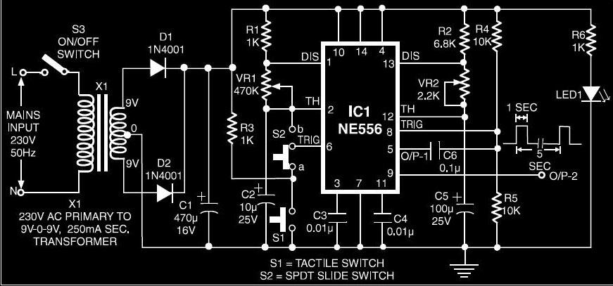
  This circuit using a dual-timer NE556 can produce 1Hz pulses spaced 5 seconds apart, either manually or automatically. IC NE556 comprises two independent NE555 timers in a single package. It is used to produce two separate pulses of different pulse widths, where one pulse initiates the activation of the second pulse.

  The first half of the NE556 is wired for 5-second pulse output. When slide switch S2 is in position ‘a’, the first timer is set for manual operation, i.e. by pressing switch S1 momentarily you can generate a single pulse of 5- second duration. When switch S2 is kept in ‘b’ position, i.e. pins 6 and 2 are shorted, timer 1 in NE556 triggers by itself.
  The output of the first timer is connected to trigger pin 8 of second timer, which, in turn, is connected to a potential divider comprising resistors R4 and R5. Resistor R1, preset VR1, resistor R2, preset VR2, and capacitors C2 and C5 are the components determining time period. Presets VR1 and VR2 permit trimming of the 5-second and 1-second pulse width of respective sections.
When switch S2 is in position ‘a’ and switch S1 is pressed momentarily, the output at pin 5 goes high for about 5 seconds. The trailing (falling) edge of this 5- second pulse is used to trigger the second timer via 0.1μF capacitor C6. This action results in momentarily pulling down of pin 8 towards the ground potential, i.e. ‘low’. (Otherwise pin 8 is at 1/2 Vcc and triggers at/below 1/3 Vcc level.) When the second timer is triggered at the trailing edge of 5-second pulse, it generates a 1- second wide pulse.
    When switch S2 is on position ‘b’, switch S1 is disconnected, while pin 6 is connected to pin 2. When capacitor C is charged, it is discharged through pin 2 until it reaches 1/3Vcc potential, at which it is retriggered since trigger pin 6 is also connected here. Thus timer 1 is retriggered after every 5-second period (corresponding to 0.2Hz frequency). The second timer is triggered as before to produce a 1-second pulse in synchronism with the trailing edge of 5-second  pulse.
   This circuit is important wherever a pulse is needed at regular intervals; for instance, in ‘Versatile Digital Frequency Counter Cum Clock’ construction project published in EFY Oct. ’97, one may use this circuit in place of CD4060-based circuit. For the digital clock function, however, pin 8 and 12 are to be shorted after removal of 0.1μF capacitor and 10-kilo-ohm resistorsR4 and R5.

Twitter Delicious Facebook Digg Stumbleupon Favorites More